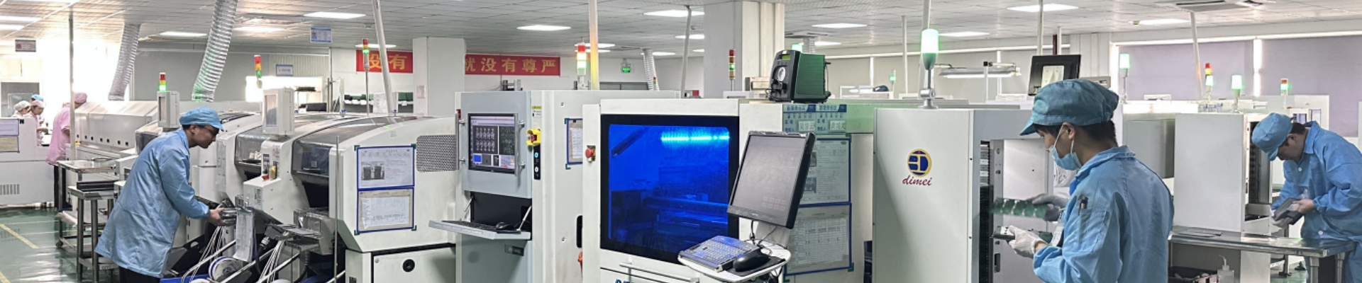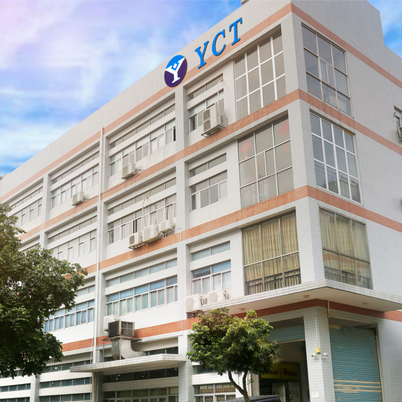
Shenzhen YCT Electronics Co ,Limited is a national high-tech enterprise established in 2009, which is committed to providing one-stop service for both samples and batch orders in PCB manufacturing, component sourcing, PCB assembly, and testing YCT currently has two production bases in Bao’an Shenzhen and Longgang Shenzhen, with 8 SMT production lines, 2 wave soldering production lines.
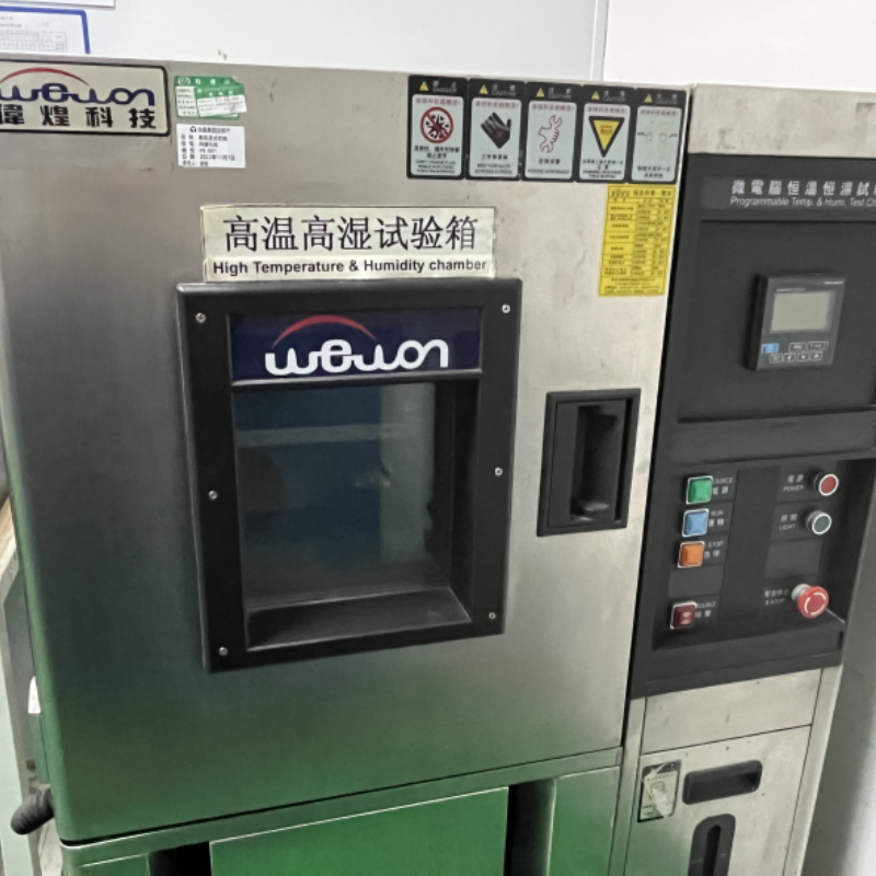
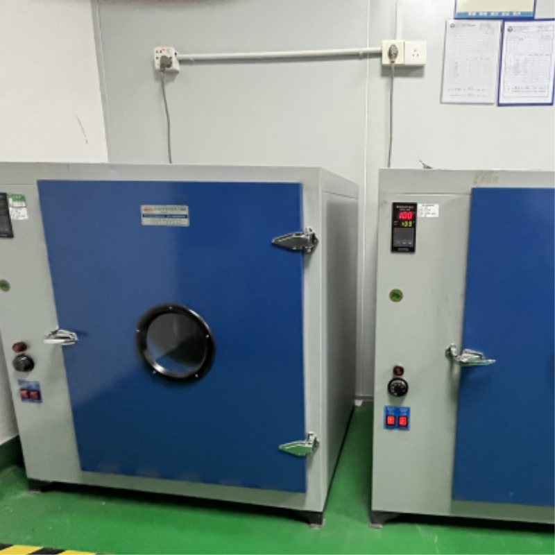
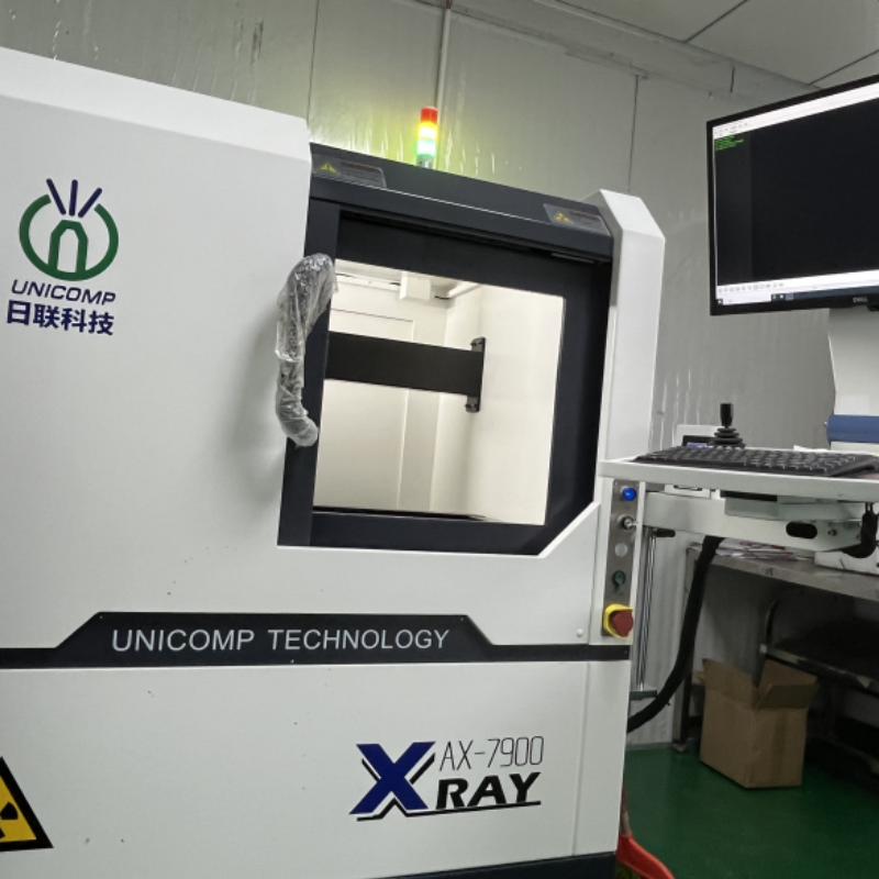
The workshop is equipped with high-end production and testing equipment including imported Panasonic high-speed SMT machines, reflow soldering, AOI, X-ray, etc., as well as reliability Testing(Hi-Temp,Low-Temp,Ordinary Temp,Humidity,Salt Spray).
Establishing and implementing a management system in accordance with standards, our company has currently passed ISO9001:2016 quality management system certification,. Through a standardized and goal-based quality management system, we can more effectively improve management effectiveness and work efficiency, and establish an effective mechanism for active self-improvement and continuous improvement, thereby providing customers with better products and services.
YCT utilizes advanced PCB manufacturing systems including automated wave soldering machines and high-precision laminators for consistent layer bonding. Our DIP equipment ensures reliable through-hole component assembly, while automated board-cutting maintains dimensional accuracy within tight tolerances. The integration of wire bonding technology supports complex circuit designs without compromising production speed.
With 10+ years in PCB fabrication, YCT’s engineers excel at troubleshooting trace peeling and misregistration through optimized press cycles. We mitigate solderability issues via controlled lamination processes and resolve undercut problems in etching through proprietary techniques. Continuous learning curve analysis refines parameters for V-cut scoring and beveling operations.
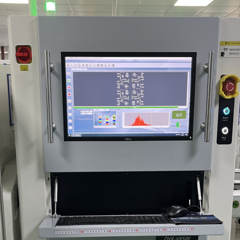
Every batch undergoes: ICT testing to detect opens/shorts AOI inspection for pinholes and nicks Ionic contamination tests for cleanliness compliance Thermal cycling and salt spray tests to validate endurance Dedicated flying probe and universal testers5 provide flexible verification for high-mix orders.
YCT combines cutting-edge technology with proven expertise to deliver high-reliability PCB solutions—backed by rigorous testing and tailored support. Our commitment to precision and customer success makes us the ideal partner for your electronics manufacturing needs.

Multi-stage inspections (AOI, flying probe tests)
Hi-Temp/Low-Temp reliability testing to validate board endurance
Compliance with traceability standards for defect prevention
DIP/SMT hybrid assembly lines for flexible configurations
Automated wire bonding for high-density interconnects
Precision V-cut scoring and beveling for edge-critical designs
Dedicated RF test support for signal integrity validation
Ionic contamination monitoring to ensure cleanliness
Transparent learning curve updates for continuous process refinement

We provide global electronic component sourcing with technical BOM analysis for genuine parts procurement. Our dual-source strategies mitigate supply chain risks while handling miniature packages (0402/0201). We offer component substitution guidance during shortages and cost optimization through quarterly market intelligence. AVL management ensures 98% on-time delivery performance for continuous production.
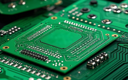
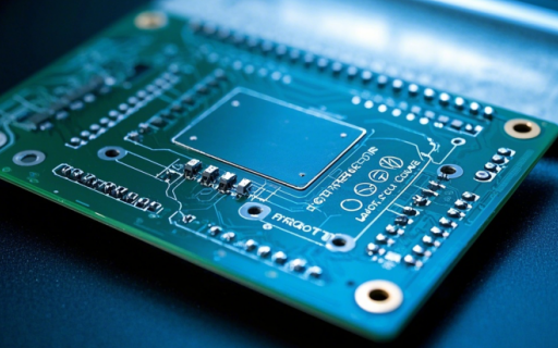
Our high-reliability PCB manufacturing supports 1-32 layer designs with ±0.075mm hole tolerance and advanced material options (Rogers, Taconic). We specialize in rigid, flex, and rigid-flex solutions including hybrid constructions with buried capacitance. Multiple surface finishes (ENIG, immersion silver, selective gold) meet diverse requirements. Every PCB undergoes electrical testing and plating quality verification.

Turnkey assembly integrates DFM analysis with precision SMT (01005 components) and through-hole assembly. We deploy 3D SPI inspection, nitrogen reflow, and selective soldering to ensure quality. Comprehensive testing includes ICT, flying probe, and functional validation. Additional services cover box build integration, failure analysis, and conformal coating for harsh environments.
Rapid prototyping delivers 2-layer PCBs in 24 hours and multilayer (12L) in 48 hours. Advanced options feature HDI technology (0.1mm traces, laser microvias) and board-on-panel validation. Engineering support includes signal integrity analysis, thermal modeling, and manufacturing risk assessment. Our 16-year expertise supports complex projects with ITAR and IATF 16949 certifications.
Our quality control system implements rigorous testing protocols to ensure PCB reliability. We perform AOI inspection and flying probe testing for defect detection, combined with VRS visual verification .