Introduction to Our Assembly Approach
We take a systematic approach to PCB assembly, emphasizing accuracy, efficiency, and traceability at every stage. Whether you need a small prototype run or large-scale production, our team is equipped to meet your exact specifications while maintaining short lead times and competitive pricing.
Step 1: Material Procurement
Our process begins with careful sourcing of all components and bare PCBs.
Trusted Suppliers: We collaborate with reliable vendors to ensure part authenticity and availability.
Quality Checks: Incoming materials are inspected and verified to catch any issues before they reach the production floor.
By focusing on top-quality materials, we minimize the risk of production delays or subpar end products.
Step 2: Solder Paste Application and Inspection
Proper solder paste application is crucial for forming strong, dependable solder joints.
Stencil Printing: We use precision stencils to apply solder paste accurately.
Solder Paste Inspection (SPI): Automated systems confirm that the deposit volume and alignment match specified tolerances, reducing the chance of defects later on.
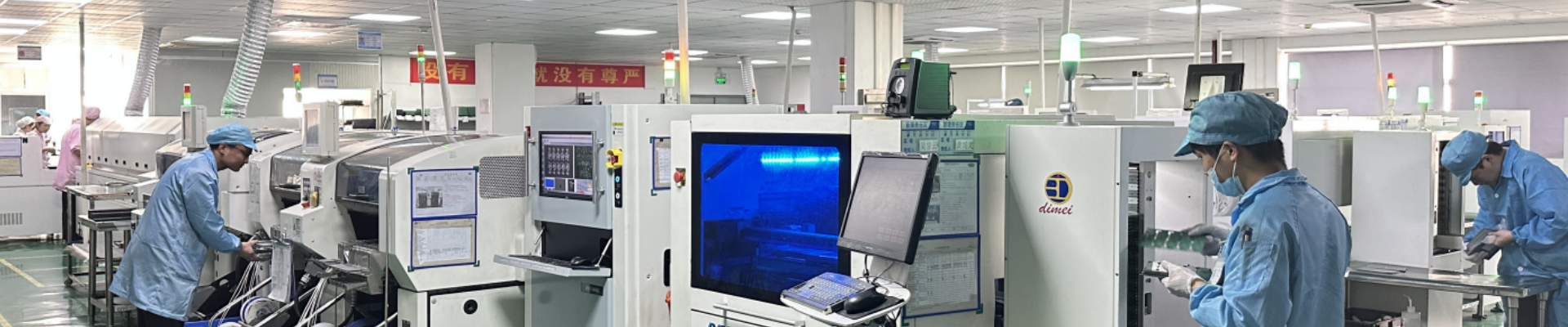
Step 3: SMT (Surface Mount Technology) Assembly
Surface Mount Technology allows us to place components quickly and accurately:
Pick-and-Place Machines: These high-speed devices position each component on the board with pinpoint accuracy.
Reflow Soldering: Once placed, the boards move through a temperature-controlled oven where solder paste melts and cools, securing components to the PCB.
At this stage, consistency is key—our equipment and fine-tuned profiles produce reliable solder joints for each board.
Step 4: THT (Through-Hole Technology) Assembly
For boards requiring through-hole components, we offer both automated and manual assembly methods:
Wave Soldering: Ideal for mass production, wave soldering bonds leads to the PCB quickly and efficiently.
Selective Soldering or Manual Insertion: Used for sensitive or unique components that demand precise care.
In either case, we ensure each lead is properly aligned and soldered, maintaining strong mechanical and electrical connections.
Step 5: Inspection and Testing
We employ multiple inspection methods to confirm quality and functionality:
Automated Optical Inspection (AOI): Verifies component placement, polarity, and solder joints through high-resolution cameras.
X-Ray Inspection: Offers a closer look at hidden joints, like those under BGAs (Ball Grid Arrays).
Functional Testing: Confirms that each assembled PCB meets the intended performance criteria by simulating real-world conditions.
This layered approach to testing minimizes the chance of hidden flaws and guarantees consistent output.
Step 6: Quality Assurance and Final Checks
Before we ship any product, our quality team performs a final evaluation:
IPC-A-610 Compliance: Each assembly is checked against industry standards for workmanship and reliability.
Documentation and Traceability: We maintain detailed records, giving you peace of mind and a clear audit trail.
By the time the boards leave our facility, we have full confidence in their performance and quality.
Our Specialized Equipment and Certifications
We stay current with industry best practices to maintain a high level of quality. Modern pick-and-place machines, reflow ovens, and wave soldering systems work together for efficient throughput. We also hold certifications such as ISO 9001 and adhere to IPC guidelines, reinforcing our commitment to consistent, high-grade results.
Industries We Serve
We adapt our PCB assembly process to match the needs of diverse industries:
Automotive: Control systems, sensor modules
Consumer Electronics: IoT devices, smart gadgets
Medical: Diagnostic instruments, patient monitoring systems
Industrial: Automation controllers, power management solutions
Telecommunications: Network equipment, RF modules
Our wide-ranging experience allows us to tackle unique challenges across each sector.
Why Partner With Us
Technical Expertise: Our skilled team handles everything from standard single-layer boards to complex multi-layer assemblies with fine-pitch components.
Cost-Effective Solutions: We work to optimize both materials and labor, balancing quality with budget considerations.
Time-to-Market Focus: Efficient processes and clear communication help you meet tight product launch timelines.
Customer-Centric Mindset: From the first inquiry to final delivery, we prioritize your satisfaction and remain transparent every step of the way.
Frequently Asked Questions
Q: How can I request a quote?
A: Send us your BOM, Gerber files, and any design notes, and our team will provide a customized quote as soon as possible.
Q: Do you have a minimum order quantity?
A: We support everything from prototypes to large-scale production, so there’s no strict minimum.
Q: What about confidentiality and IP protection?
A: We take your intellectual property seriously. NDAs can be signed to safeguard sensitive information.
Q: Can you handle design modifications if needed?
A: Yes, we can offer DFM (Design for Manufacturability) advice and minor design tweaks to enhance production efficiency.