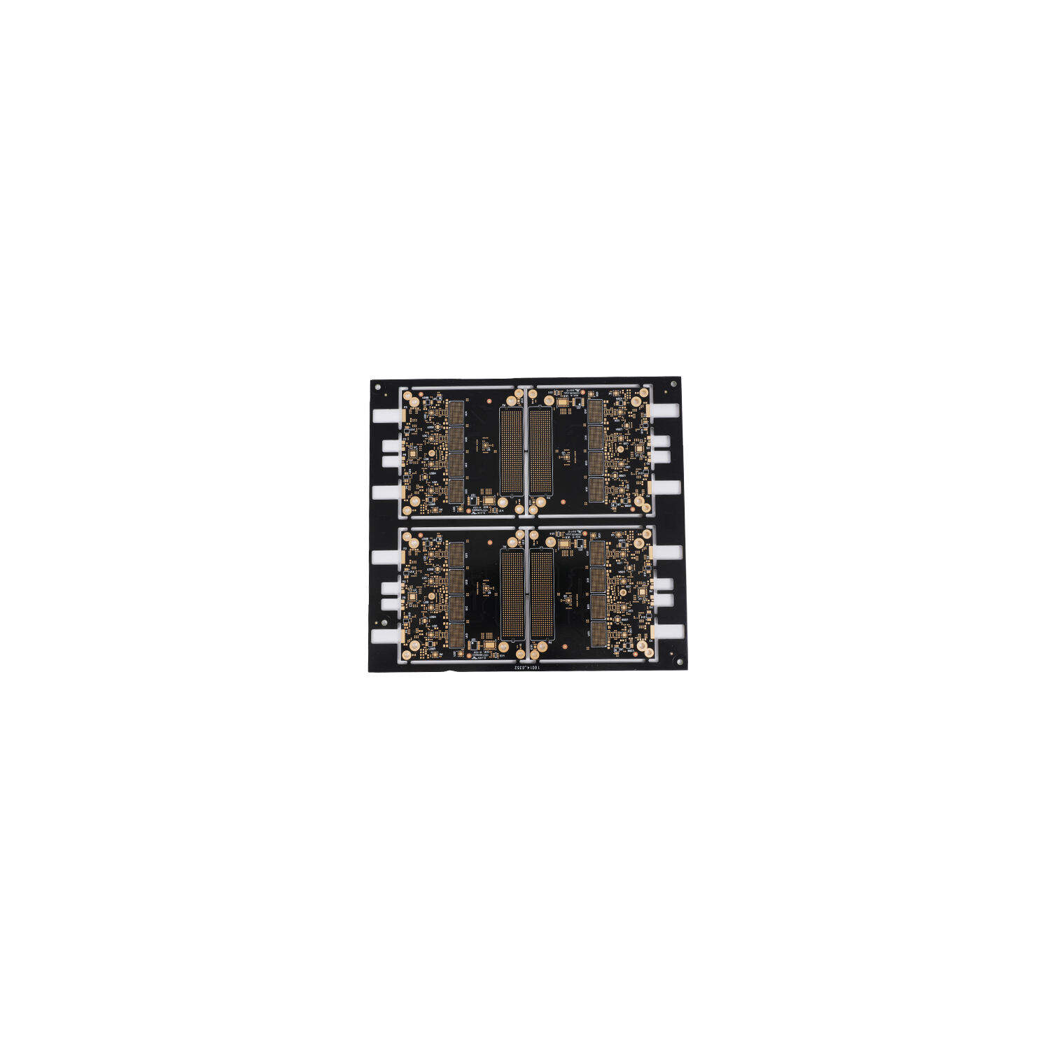
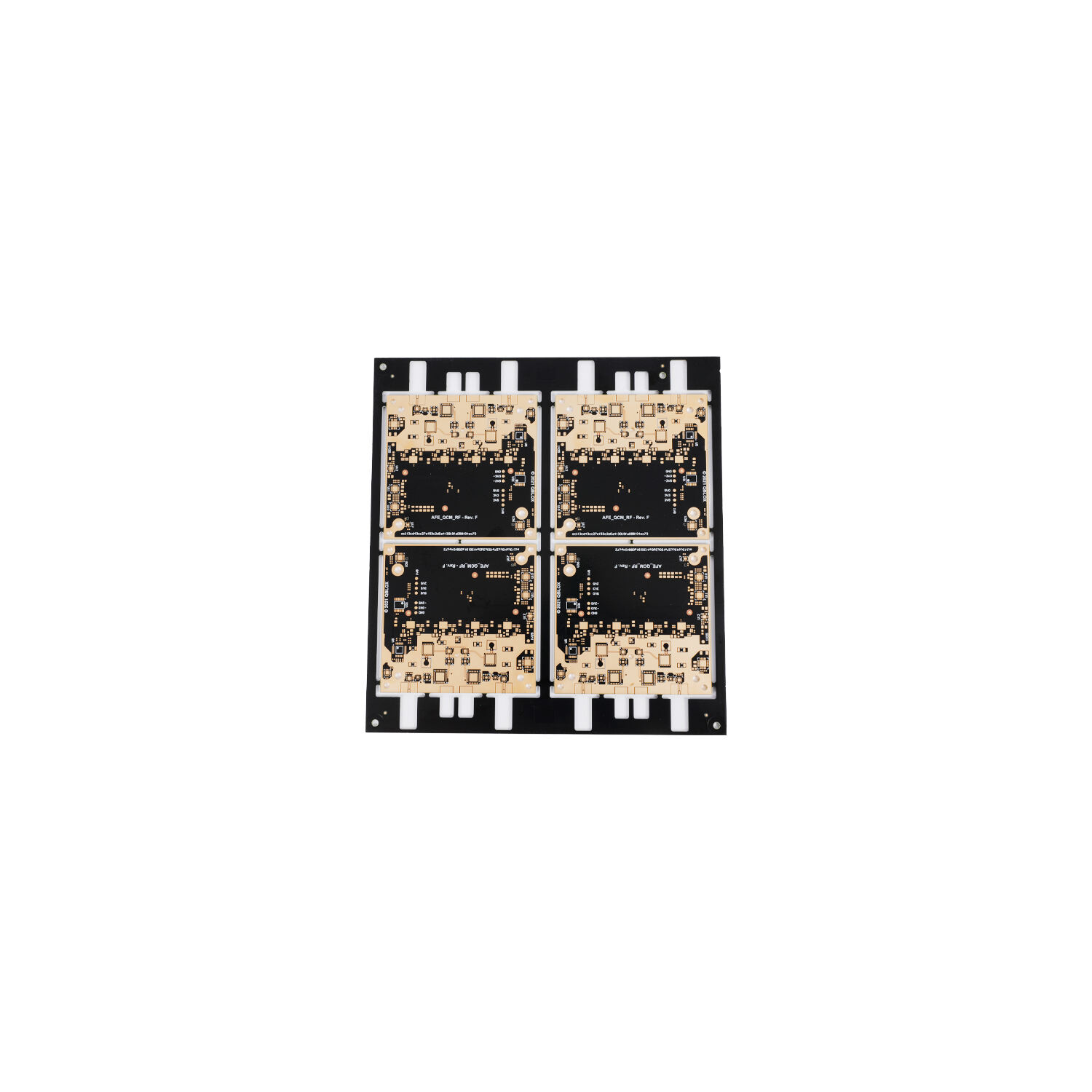
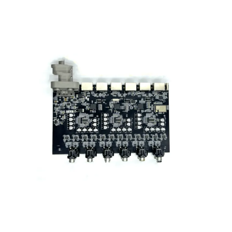
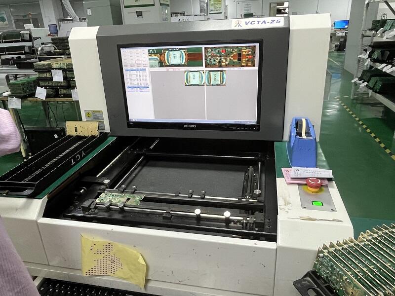
SMD (SurfaceMount Device) PCB assembly is the cornerstone of modern highdensity electronics, enabling precise placement of surfacemount components onto PCB surfaces. The process begins with solder paste printing using laseraligned stencil printers (±12.5μm accuracy), depositing SnAgCu paste onto pads for 01005 passives to 1mm pitch BGAs. Highspeed pickandplace machines (100,000+ placements/hour) use vision systems to achieve sub50μm positional accuracy, even for 0.3mm pitch finepitch components. Reflow soldering follows, with nitrogenenhanced ovens controlling thermal profiles to melt paste and form reliable joints (tensile strength ≥50N for 0402 components), while minimizing oxidation. Postreflow, AOI systems detect 99% of surface defects—solder bridges, missing components— and Xray inspection verifies hidden joints in BGAs/CSPs. SMD assembly supports advanced techniques like doublesided placement, 3D component stacking, and embedded passives, critical for miniaturized devices such as smartphones and wearables. Manufacturers offer DFM support to optimize pad designs and spacing, ensuring high firstpass yields (≥98%) and compatibility with leadfree (RoHS) standards.