PCBA Manufacturers Mass Production PCB Assembly Providers

Get a Free Quote

Our representative will contact you soon.
Email
Mobile/WhatsApp
Name
Company Name
Message
0/1000
Attachment
Please upload at least an attachment
Up to 3 files,more 30mb,suppor jpg、jpeg、png、pdf、doc、docx、xls、xlsx、csv、txt

Multi Layer PCB Assembly Solutions for Your Electronics Needs

Welcome to Shenzhen YCT Electronics Co., Limited, your trusted partner for multi-layer PCB assembly. Established in 2009, we are a national high-tech enterprise committed to providing a comprehensive one-stop service for PCB manufacturing, component sourcing, assembly, and testing. With state-of-the-art facilities in Shenzhen and advanced production lines, we ensure high-quality assembly services tailored to meet your specific requirements, whether for prototypes or mass production.
Get A Quote

Advantages of the product

Cutting-Edge Technology

Our assembly process utilizes high end production and testing equipment, including imported Panasonic high speed SMT machines and advanced reliability testing methods. This ensures that every multi layer PCB we produce meets the highest industry standards, providing you with reliable and durable products.

Related products

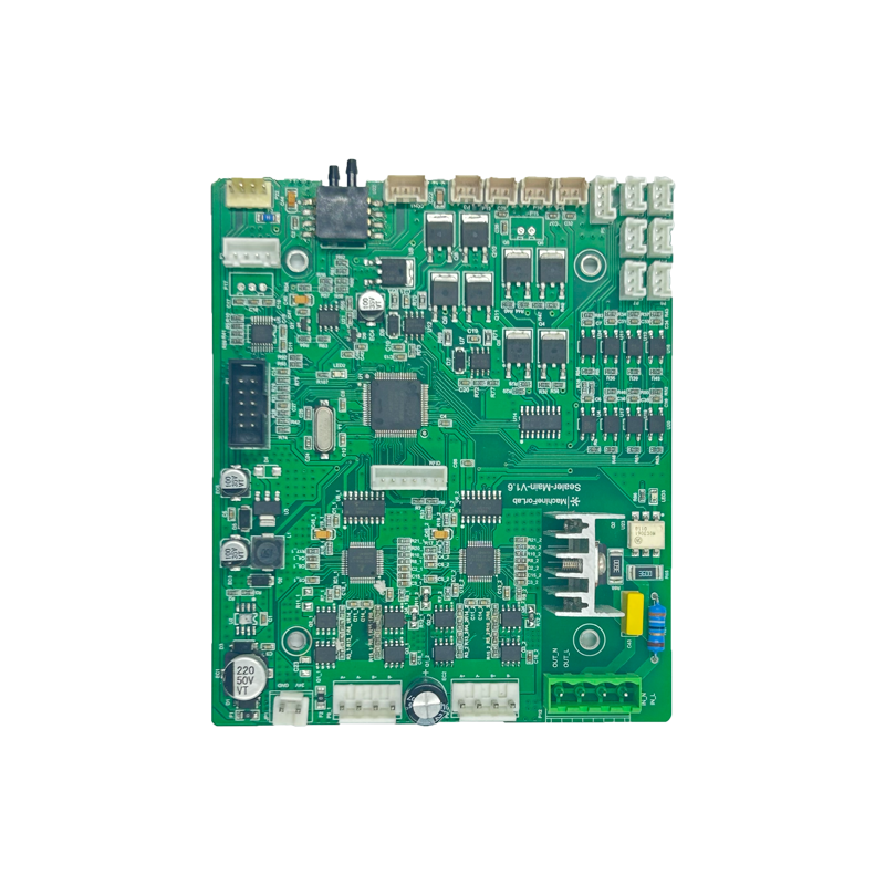
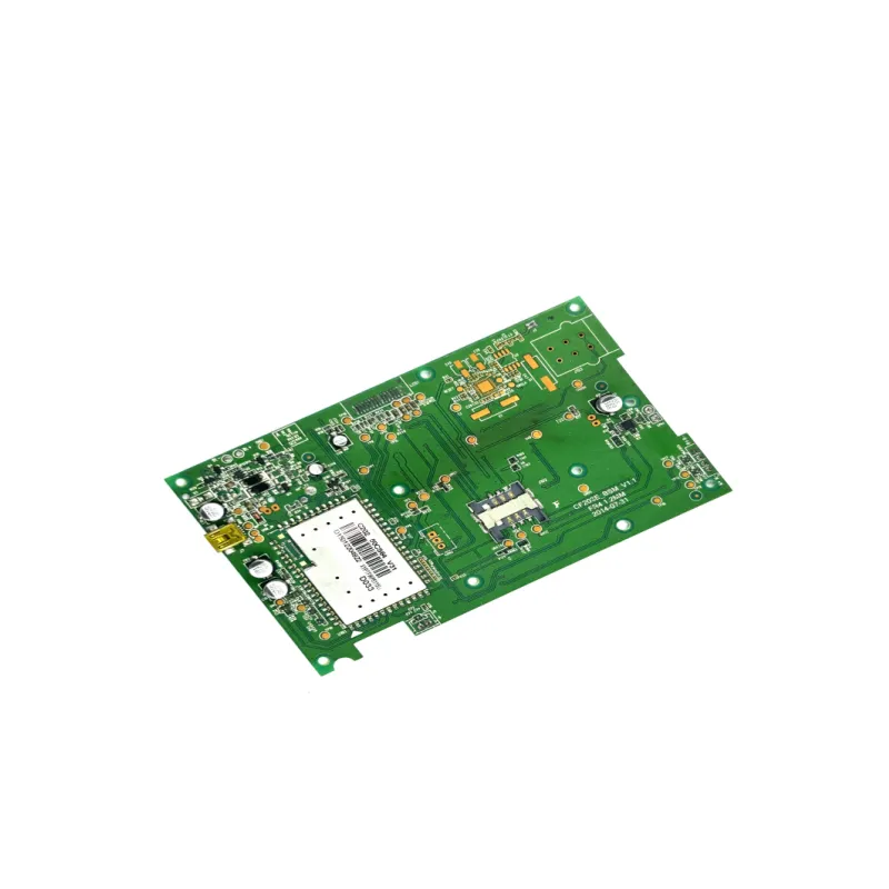
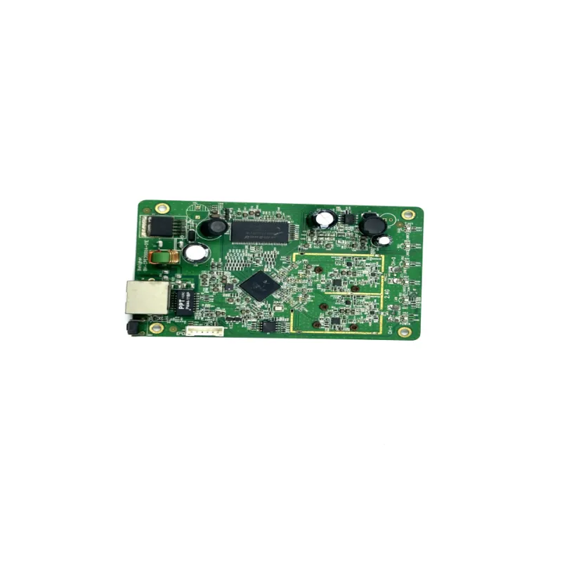
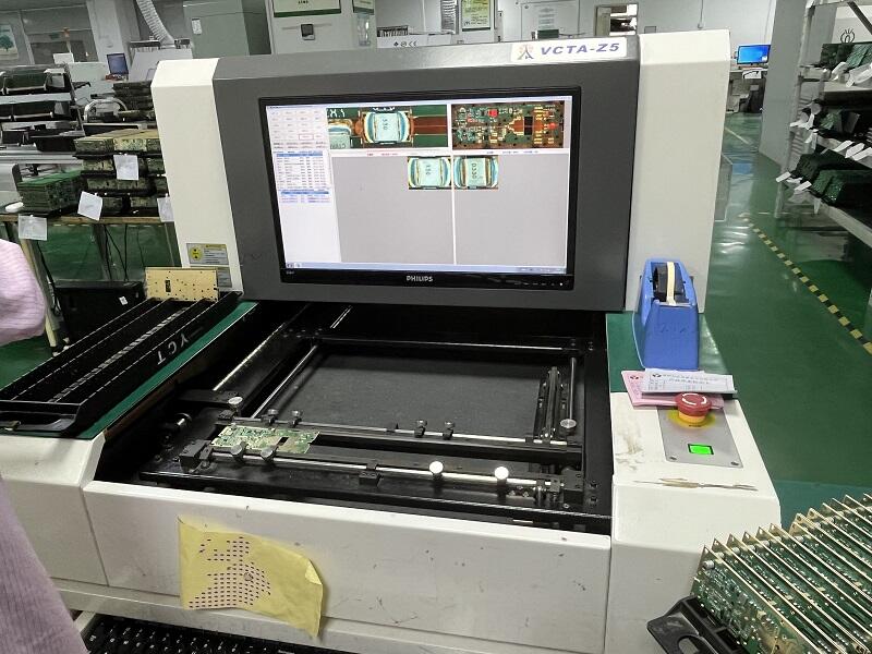
Multi layer PCB assembly is a specialized area within the PCB manufacturing and assembly industry, catering to applications that require high density interconnects, complex routing, and advanced electrical performance. A multi layer PCB consists of multiple layers of conductive traces separated by insulating materials, which allows for a greater number of components to be integrated and more intricate circuit designs to be realized. The assembly process for multi layer PCBs is more complex compared to single or double layer boards. It begins with the careful fabrication of each individual layer, which involves processes such as copper deposition, photo imaging, and etching. These layers are then precisely aligned and laminated together using high pressure and high temperature processes to form the multi layer structure. After lamination, vias are drilled and plated to create electrical connections between the different layers. When it comes to component assembly on multi layer PCBs, the same SMT and THT techniques are employed, but with additional considerations. Due to the higher component density, precise component placement is even more critical to avoid interference and ensure proper electrical connections. High frequency applications often require multi layer PCBs with controlled impedance, which means that the trace widths, spacing, and layer stack up must be carefully designed and maintained during assembly. Testing multi layer PCBs is also more challenging. In addition to the standard AOI and X ray inspection methods used for single and double layer boards, multi layer PCBs may require more in depth electrical testing to verify the integrity of the inter layer connections. This can include techniques such as in circuit testing (ICT) and flying probe testing, which can detect open circuits, short circuits, and incorrect component values. Multi layer PCB assembly is widely used in various high tech industries, such as telecommunications, aerospace, military, and high performance computing. In telecommunications, multi layer PCBs are used in base stations and network equipment to handle high speed data transmission. In aerospace and military applications, they are required to meet strict reliability and environmental standards, as they are used in critical systems such as avionics and missile guidance. Overall, multi layer PCB assembly is a highly specialized and demanding field that requires advanced manufacturing techniques, strict quality control, and in depth technical expertise.

Frequently Asked Questions

What value do turnkey PCBA manufacturers offer?

From design optimization to after-sales support, turnkey providers manage the entire supply chain, allowing clients to focus on product innovation rather than production logistics.

Related Articles

E-Test

22

Apr

E-Test

View More
 Flying Probe Test(FPT)

22

Apr

Flying Probe Test(FPT)

View More
Pcb Layout

11

Apr

Pcb Layout

View More
Spring Camping

16

Apr

Spring Camping

View More

customer evaluation

Vaughn

YCT's high-volume PCBA capabilities reduced our per-unit cost by 18%. The automated testing and lean processes improved our bottom line.

Get a Free Quote

Our representative will contact you soon.
Email
Mobile/WhatsApp
Name
Company Name
Message
0/1000
Attachment
Please upload at least an attachment
Up to 3 files,more 30mb,suppor jpg、jpeg、png、pdf、doc、docx、xls、xlsx、csv、txt
Advanced Manufacturing Capabilities

Advanced Manufacturing Capabilities

Our state of the art facilities are equipped with the latest technology, ensuring high precision and quality in multi-layer PCB assembly. This capability allows us to handle complex designs and large volumes efficiently, making us a leader in the industry.
Tailored Solutions for Diverse Applications

Tailored Solutions for Diverse Applications

We understand that each project is unique. Our team works closely with clients to develop customized multi-layer PCB assembly solutions that cater to specific requirements, ensuring optimal performance and reliability in various applications.
Commitment to Quality and Reliability

Commitment to Quality and Reliability

Our rigorous testing protocols and quality assurance processes ensure that every multi-layer PCB assembly we deliver is reliable and meets the highest standards. We are dedicated to providing products that you can trust for your electronic devices.