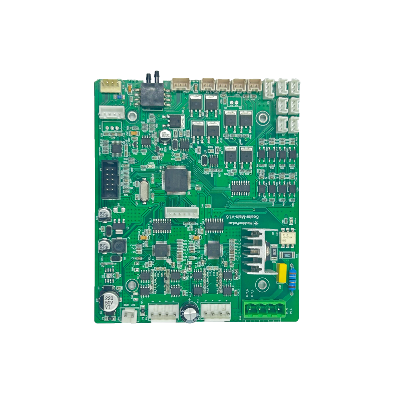
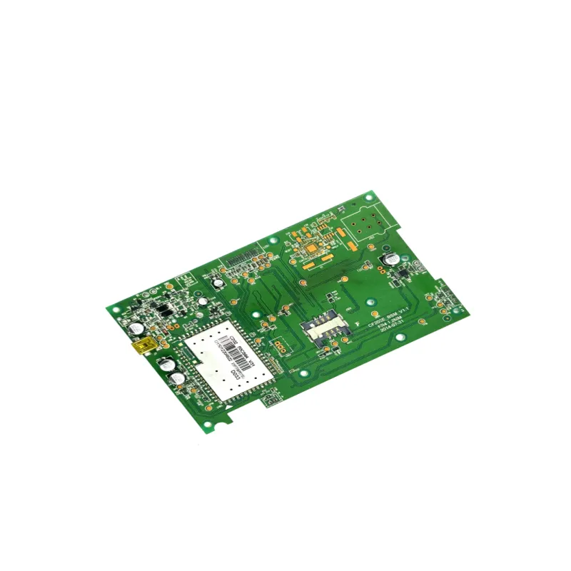
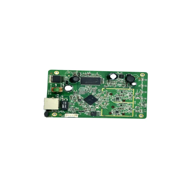
Printed Circuit Board Assembly (PCBA) is the critical manufacturing phase where raw materials are transformed into functional electronic systems, requiring a blend of technical precision, process discipline, and innovation. The PCBA journey starts with meticulous planning, including BOM validation, design rule checking, and production scheduling. Component preparation involves drying moisture sensitive devices (MSDs) in controlled environments and confirming part numbers against the BOM to prevent assembly errors. Surface mount assembly dominates modern PCBA, with automated lines achieving remarkable speed and accuracy. Solder paste is applied with precision printers (±10μm thickness variation), components are placed with vision guided robots (±25μm positional accuracy), and reflow ovens use zone controlled heating to create uniform solder joints. Through hole assembly, while less common, remains essential for high power components, with wave soldering systems capable of processing thousands of boards per hour. Testing is integral to PCBA, with AOI detecting 99% of surface defects, X ray systems visualizing hidden solder joints, and functional testers verifying complex circuit behavior. Advanced PCBA facilities also employ in circuit testers with bed of nails fixtures for comprehensive netlist verification, ensuring no open circuits or shorts go undetected. As electronics become more sophisticated, PCBA adapts to new challenges like miniaturization (01005 components, 0.25mm pitch BGAs), thermal management (metal core PCBs, heat sinks), and environmental resilience (conformal coating, underfill). PCBA is thus not just a process but a dynamic field driving innovation in every industry that relies on electronics, from consumer gadgets to critical infrastructure.