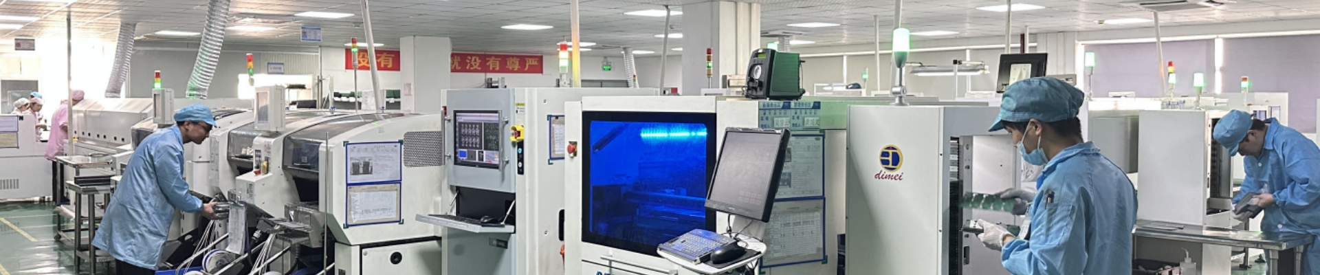
Introduction
In the world of PCB assembly, ensuring that every electrical path works exactly as intended is critical. It’s not enough for a board to look good or have properly aligned components—if the circuit doesn’t perform electrically, the board is effectively useless. That’s where the E-Test, or Electrical Test, becomes indispensable.
E-Testing is a mandatory step in the quality control process for PCB assembly. It checks the integrity of all electrical connections and confirms the board meets design specifications. Whether you're building a simple LED circuit or a multi-layer motherboard, the E-Test is the final gatekeeper before the board moves on or reaches the customer.
Think of it as an electrical polygraph—it confirms that the circuit isn’t just visually correct, but also telling the truth electrically. By detecting short circuits, open circuits, and verifying correct routing, E-Test minimizes the risk of shipping boards that will fail in the field.
What Is E-Test in PCB Manufacturing?
E-Test stands for Electrical Test, a process that confirms every conductive trace on a PCB is functioning as intended. It specifically checks:
- Current flow where it’s supposed to (continuity)
- No current flow where it shouldn’t (isolation)
Especially for multi-layer or high-density boards, manufacturing errors may be invisible to the naked eye or even advanced AOI/X-ray systems. E-Test, by applying voltage and measuring current flow, pinpoints these hidden faults.
In many operations, E-Test is done on bare boards before assembly and repeated post-assembly to verify solder joints and ensure no board damage occurred during production.
Why Electrical Testing Is Crucial in PCBA
Skipping E-Testing is akin to building a car and never starting its engine—you’ll never know if it truly works. Here’s why E-Testing matters:
- Detects Manufacturing Defects: Identifies shorts, opens, and misrouted nets.
- Prevents Product Failures: Minimizes the likelihood of field returns or malfunctions.
- Boosts Customer Trust: Demonstrates reliability and adherence to high-quality standards.
- Reduces Returns and RMAs: Decreases warranty claims and maintains brand reputation.
In short, E-Testing ensures you’re not just assembling boards, but guaranteeing their reliability.
Understanding the Electrical Test Process
How does an E-Test work? Essentially, voltage is applied to a PCB’s conductive traces while current is measured. By performing this check on each net, the system confirms:
- Continuity (traces are complete and carry current)
- Isolation (no unintended connections between unrelated nets)
These measurements are performed by specialized machines with test probes. The probes contact test pads or vias, then inject current to see if the measured result aligns with the design netlist.
■ Test Data
The system compares the electrical performance against the netlist, a digital map of expected connections.
■ Pass/Fail Logic
Boards pass if current flows as planned and meets resistance tolerances. Any discrepancies result in a fail, flagging the board for rework.
Flying Probe vs. Bed of Nails Testing
Electrical testing typically uses one of these two main approaches:
• Flying Probe Testing
– Multiple moving probes individually contact different points on the board.
– Flexible for different designs; lower setup cost but slower cycle times.
• Bed of Nails Testing
– Custom fixture with spring-loaded pins contacting all test points simultaneously.
– Ideal for high-volume production; faster testing but higher initial fixture costs.
Choose flying probe for lower volume or frequent design changes, and bed of nails for speed in mass production.
Key Parameters Checked During E-Test
When a PCB goes through an E-Test, several parameters ensure it’s electrically robust:
1. Continuity
– Confirms complete paths between intended points, factoring in solder joints and possible breakages.
2. Isolation
– Ensures no unintended shorts between separate circuits, a critical check for dense boards with tight spacing.
3. Resistance Measurement
– Highlights weak or corroded connections and identifies areas with excessive or insufficient solder.
4. Advanced Capacitance/Inductance
– Useful for high-frequency or RF boards where signal integrity is paramount.
5. Voltage Drop & Current Limits
– Monitors how current behaves under load, detecting intermittent issues or hidden damage.
Types of Electrical Tests for PCB Assemblies
Not all electrical tests are identical. Depending on production stage and complexity, various testing approaches are applied:
1. Continuity Testing
– Validates that electricity can flow from point A to B, ensuring no broken connections.
2. Isolation Testing
– Ensures no short circuits exist where nets should remain separate.
3. Power-Up Testing (Functional E-Test)
– Applies real operating power to see if voltages, currents, and components function correctly. Often overlaps with In-Circuit Testing (ICT) or full Functional Testing (FCT).
Equipment and Tools Used in E-Test
E-Testing demands specialized tools:
- Test Fixtures & Probes
– Bed-of-nails fixtures for high-volume speed or flying probes for flexibility.
– Precise alignment and robust design are crucial.
- Test Software & Automation
– Advanced software takes in your netlist, automates test sequences, and logs failures.
– Integration with MES and analytics platforms can refine processes long-term.
- Integration with AOI & ICT
– E-Test complements Automated Optical Inspection (AOI) and In-Circuit Testing (ICT), forming a robust quality system.
– This full-cycle approach catches both visual and electrical flaws.
Benefits of E-Test in PCB Assembly
E-Testing adds substantial value to any PCB assembly workflow:
1. Guaranteeing Circuit Integrity
– Confirms every trace and connection aligns with the original design, essential for boards in critical applications.
2. Reducing Field Failures & RMAs
– Detects hidden electrical issues early, slashing the costs and reputational damage of product returns.
3. Enhancing Customer Confidence
– Demonstrates a solid commitment to quality. Many clients demand 100% E-Test certification.
4. Support for Continuous Improvement
– Captured test data reveal patterns over time, guiding design refinements and better manufacturing processes.
Conclusion
In today’s fast-paced electronics landscape, product reliability is essential. While AOI and other inspections ensure physical correctness, only an electrical test can definitively confirm performance. From spotting shorts and opens to validating each connection, E-Test offers peace of mind that your PCBs are truly production-ready.
Whether you choose flying probe testing for flexibility or bed-of-nails for speed, every board should get its final electrical stamp of approval. Although setting up E-Testing requires investment and expertise, the returns—fewer field failures, stronger brand reputation, and greater customer satisfaction—are well worth it.
FAQs
1. What is the difference between E-Test and Functional Test?
– E-Test verifies electrical continuity and isolation. Functional Testing powers the board to simulate real operating conditions.
2. Can E-Test catch all types of PCB defects?
– No, E-Test targets electrical faults. Visual or component placement issues are best handled by AOI and other inspections.
3. How much does E-Testing add to PCB manufacturing cost?
– Costs depend on board complexity and the testing method—flying probe has lower setup costs; bed-of-nails is faster at scale.
4. Is E-Test required for prototype PCBs?
– Yes. Even in early development phases, E-Test can prevent costly rework and unpredictability later, especially for complex boards.
5. What happens if a board fails E-Test?
– It is flagged for rework or scrapped, depending on the fault’s severity. Detailed logs guide technicians on remediation steps.