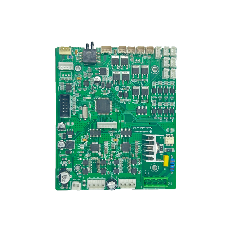
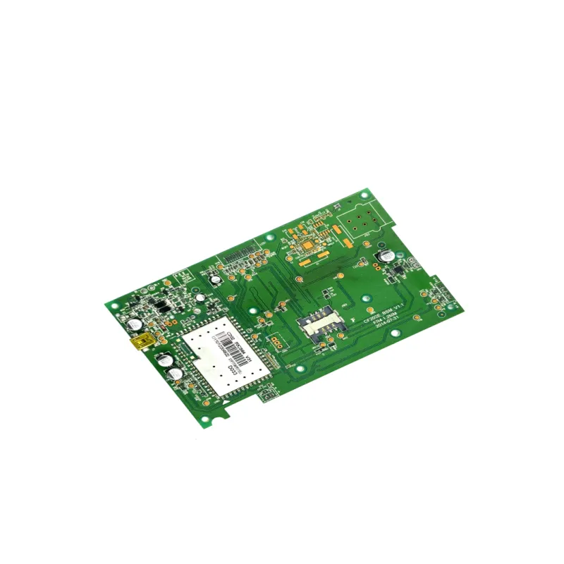
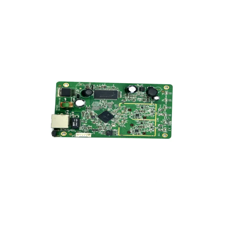
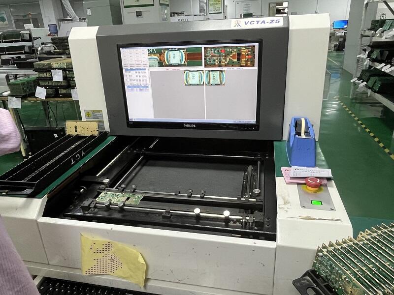
PCB printing and assembly (fabrication + assembly) is an integrated process that combines the creation of the PCB substrate with the integration of electronic components, offering end to end manufacturing under one roof. This approach enhances coordination, reduces lead times, and improves quality control. PCB printing (fabrication) begins with gerber data processing, where design files are converted into manufacturing instructions. The process includes copper plating, photoimaging, etching, and drilling, with advanced capabilities like HDI lamination, microvia formation, and impedance control. Fabrication engineers optimize stackups for signal integrity, ensuring that the finished PCB meets the electrical and mechanical requirements of the design. Upon fabrication, the PCB moves to assembly, where components are placed and soldered using SMT, THT, or hybrid techniques. Integrated providers leverage in house fabrication data to streamline assembly, such as using drilled hole data for component insertion or solder mask details for placement verification. This eliminates errors from external data transfer and ensures design intent is preserved. Quality control benefits from the integrated workflow, as fabrication defects (e.g., misdrilled holes, trace shorts) can be caught before assembly, and assembly issues (e.g., component misplacement, solder bridges) are linked to fabrication parameters for root cause analysis. Combined with advanced testing methods, this results in higher first pass yields and reduced rework costs. PCB printing and assembly providers are ideal for clients seeking a simplified supply chain, offering 一站式 services from design to delivery. They excel in handling complex boards with tight tolerances, ensuring seamless integration of fabrication and assembly for optimal performance and reliability.