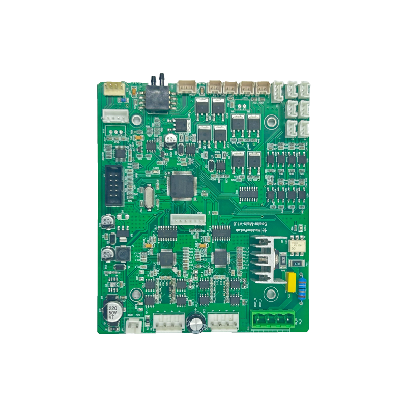
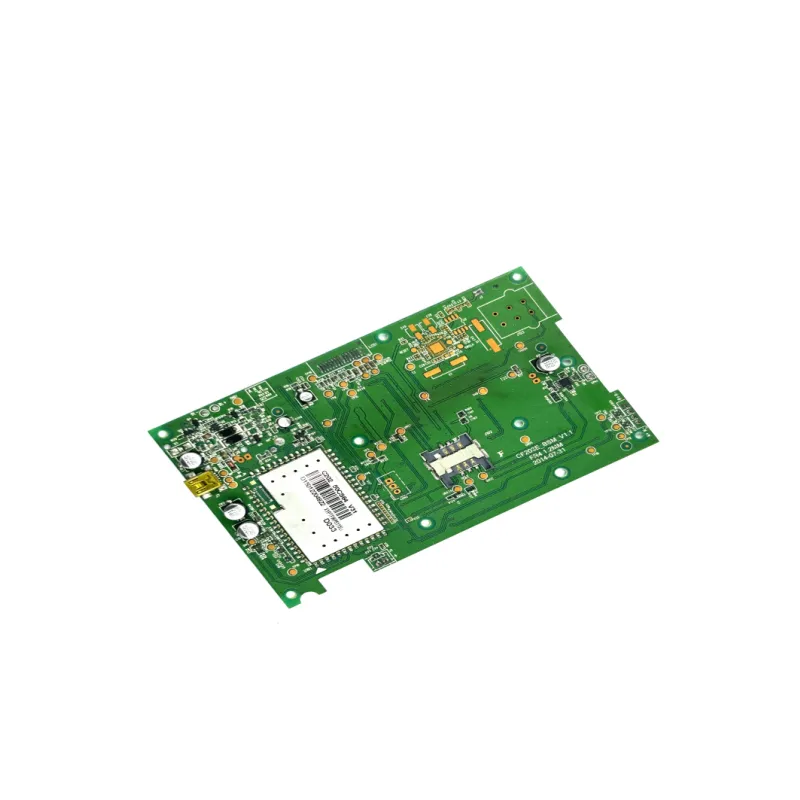
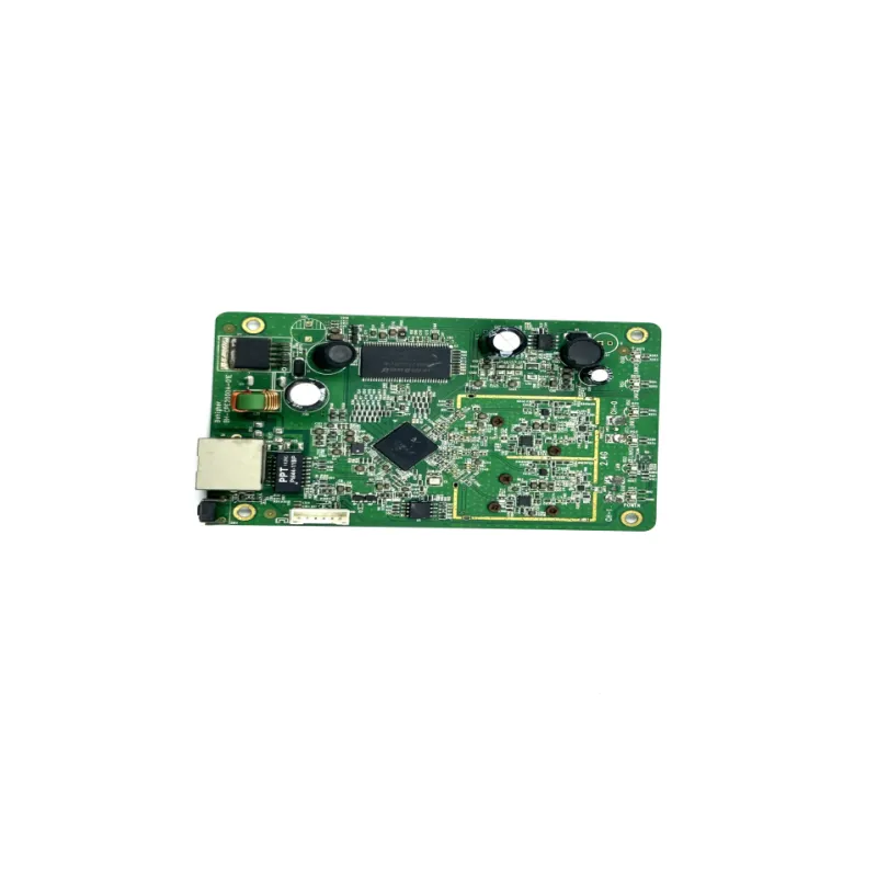
PCBA (Printed Circuit Board Assembly) is the core process of integrating bare PCBs with electronic components to create functional assemblies, forming the backbone of all electronic devices. This multidisciplinary field requires expertise in materials science, precision engineering, and quality assurance. The PCBA workflow begins with material preparation, where PCBs are inspected for dimensional accuracy and surface finish, and components are validated for moisture sensitivity and package integrity. SMT assembly starts with solder paste printing, using laser aligned stencil printers to achieve ±12.5μm placement accuracy, critical for fine pitch components. Pick and place machines then position components with vision systems ensuring sub 50μm positional accuracy, even for 0201 or smaller parts. Reflow soldering employs profile optimization software to match component thermal requirements, preventing thermal stress or cold joints. For THT components, wave soldering with nitrogen enhanced systems reduces oxidation, improving joint reliability. Mixed technology boards undergo sequential processing, with SMT components reflowed first before THT insertion and wave soldering. Post assembly, non destructive testing methods are employed: AOI for surface defects, X ray for hidden solder joints, and ICT for netlist verification. Functional testing simulates real world operating conditions, checking for signal integrity, power consumption, and protocol compliance. Advanced PCBA providers also offer conformal coating, underfill, and potting services for environmental protection in harsh applications. As electronics miniaturize and complexity grows, PCBA evolves to handle 3D packaging, embedded components, and heterogeneous integration. Mastery of these technologies ensures PCBA remains the cornerstone of modern electronics manufacturing, enabling everything from smartphones to industrial robots.